Intel iAPX 432
Computer Science 460
Final Project
Group 4: David King, Liang Zhou, Jon Bryson, David Dickson
April 15, 1999
TABLE OF CONTENTS
INTRODUCTION *
ARCHITECTURAL CLASSIFICATION *
INTENDED APPLICATIONS (S) *
INSTRUCTION SET *
GENERAL *
DATA TYPES *
ADDRESSING MODES/FORMATS *
HIGH-LEVEL LANGUAGE SUPPORT *
OPERATING SYSTEM SUPPORT *
PROCEDURE CALLING SUPPORT *
TASK SWITCHING *
CPU RESOURCES *
REGISTER SET *
FUNCTIONAL UNITS *
INTERNAL BUSES *
CONTROL UNIT *
EXTERNAL BUS STRUCTURE *
INSTRUCTION FETCH AND EXECUTION *
MEMORY SYSTEM *
OVERVIEW *
ADDRESS TRANSLATION *
CACHE *
INTERLEAVING *
MEMORY MANAGEMENT *
SUPPORT FOR SHARING MEMORY BETWEEN PROCESSORS *
INTER-PROCESSOR COMMUNICATIONS NETWORKS *
I/O SYSTEM *
SYSTEM SPEED *
EXCEPTION PROCESSING *
INTERRUPTS AND TRAPS *
CONCLUSION *
REFERENCES *
In 1975, Intel began work on a microcomputer system project. The goals for this system were large-scale computational power, incremental performance capacity, highly dependable hardware and software, and increased programmer productivity.
Six years later, in 1981, Intel announced a new processor:
The development of the iAPX 432 system might be considered the most significant architectural development of 1970’s; it was an ambitious super-CISC, object-oriented VLSI microprocessor. It achieved the integration of software operations in hardware by having many operating system functions in hardware and microcode (it provides a collection of mechanisms in hardware, leaving the selection of policies to the software). This was partially due to an attempt to implement in silicon a system similar to Carnegie-Mellon’s Hydra operating system. The 432 employs protection and addressing concepts to limit the consequences of errors, has a heavy emphasis on encouraging good software-structuring practices, has aids for software testing and debugging, and has mechanisms that reduce the complexity of operating systems and other system programs. (II, 335)
The 432 challenged the limits of the technology available at the time; it was so complex that 3 chips (4 in the final release) were required to contain all the hardware. The 432 failed commercially as a processor but was a major learning experience for Intel; it was a success of sorts that the final product performed correctly.
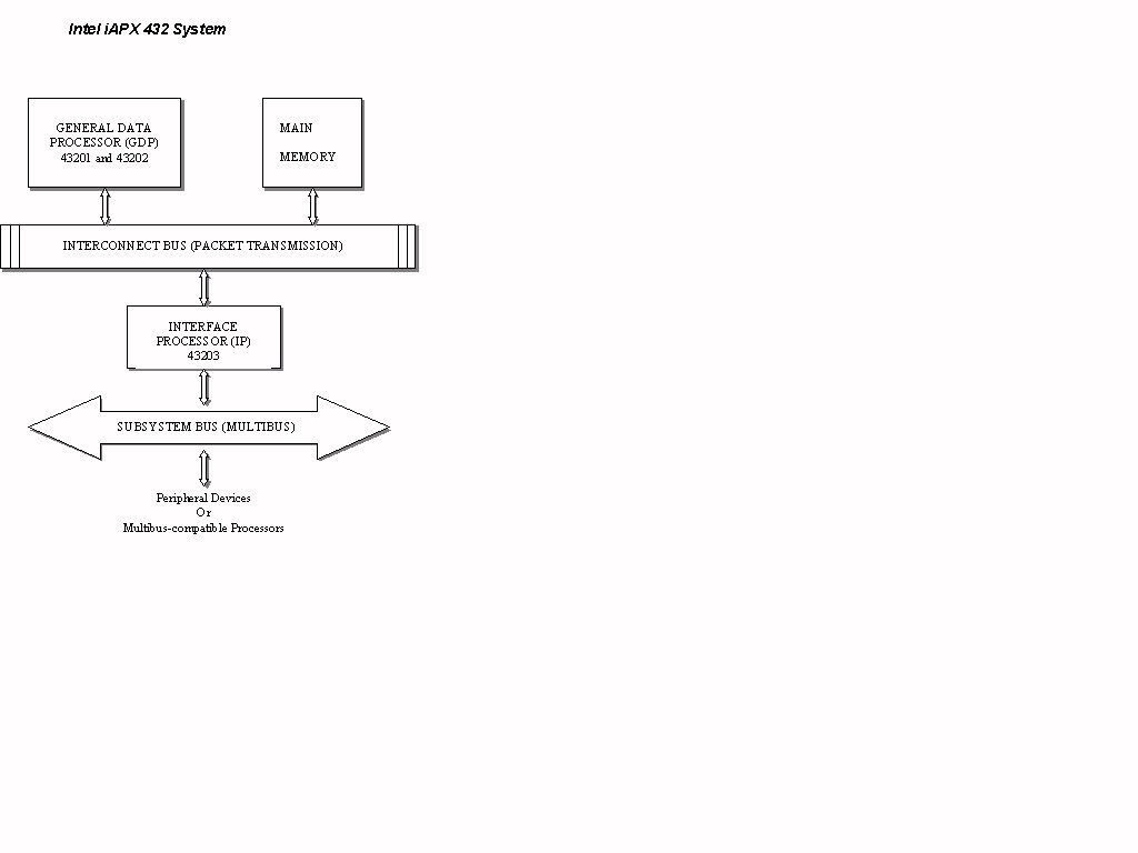
The Intel iAPX 432 was a "micromainframe" 32-bit microcomputer system composed of three chips (see Figure 1). Two of the chips, the 43201 and the 43202, made up the general data processor (GDP). The third chip, the 43203, was the interface processor (IP). All three of the 64-pin chips were manufactured with the semiconductor process (high-density metal oxide semiconductor: HMOS) using a quad in-line package (QUIP). Each chip used less than 2.5 watts from a single 5-volt supply. The iAPX 432, having a combined total of around a quarter of a million devices, fell into the VLSI category of integrated circuits (III, 601). The 432 had a MIMD, stack-based architecture, which was designed to be a multiprocessor system that could accommodate a total of six processors, each either a GDP or IP.
The Intel iAPX 432 was specifically designed to facilitate the development of large, reliable, software-intensive applications (I, 170). Applications such as patient monitoring, nuclear power plant instrumentation and control, and factory/office systems are just a few examples of systems that demand this type of software (I, 172). With the iAPX 432 having such great hardware capabilities, its use was also favored in areas such as database and transaction processing (I, 167).
The iAPX 432 was intended for use with the Ada programming language; both Ada and the iAPX 432 were developed at about the same time to solve similar problems. Later iAPX processors, including all releases of the 432, were designed explicitly for Ada while earlier iAPXs simply had an Ada-like assembly language (IV, 47).
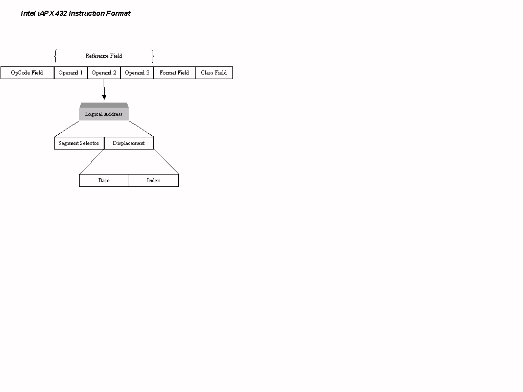
The iAPX 432 had 230, four-field instructions. The first two fields, the class field and the format field, specify the number of operands in the instruction and how they should be accessed. The third field is the reference field; it contains the logical addresses of the operands. The operands can be scalars, vectors, or records and can number from zero to three. The last field specifies the operator (I, 162) (see Figure 2). The instruction set is fully symmetric in that all addressing modes are available for all operands and all operators exist for all data types. Instructions are stored in a special memory segment and are read in 32-bit sections as a stream (III, 603). Instructions are bit variable covering a range from 6 up to and beyond 300 bits in length using Huffman encoding (I, 171).
Data manipulation can take place in the form of eight-bit characters, ordinals (16 and 32-bit), integers (16 and 32-bit), floating-point variables (32, 64, and 80-bit), bit strings, arrays, records, or "objects." The longest supported data type is the extended precision floating point type. In the iAPX 432, this type is an 80-bit temporary real data type, which is defined in the IEEE floating-point standard. The aforementioned "objects" are treated as single entities and their internal organization is hidden and protected from other hardware procedures. These objects have their own sets of instructions for direct manipulation, just as the high-level language objects of C++ and Ada do.
Some of the hardware-defined objects are as follows: processor (representing the physical processors), process (representing the individual computing tasks), context (representing the activation of a program unit), dispatching-port (a queue that provides a stream of work for a set of processors), and communications-port (supporting inter-process communication and synchronization). Objects have supported messages: process messages (SEND, WAIT), context (CALL, RETURN), storage pools (ALLOCATE, TYPE), and processes (SCHEDULE, DISPATCH). Objects allow users (or the operating system) to conceptualize their own virtual machines. Using objects as described above gives way to simplified multiprogramming and multiprocessing (I, 160).
The iAPX 432 has four addressing modes:
Base and indexed direct is for accessing scalars. Base indirect and indexed direct is used to access records. Base direct and indexed indirect is used for accessing static arrays. Finally, base and indexed indirect is used for accessing dynamic arrays (I, 163).
The Intel iAPX 432 was designed to support the Ada programming language to allow for easier creation of highly dependable software (I, 157). Ada provides object-orientated programming, modular programming support, compile time error checking, and configurable run-time error checking (I, 172). The 432’s machine language implements most of the features of Ada, including multiprocessing support for primitives (threads) (IV, 56). Sections of the iAPX 432’s process management mechanisms are conformed to follow the tasking model in the Ada language (II, 336). The emphasis on Ada turned out to be a mistake; everyone ignored the military’s attempt to make it the primary language. The unpopularity of Ada was second to speed as a main reason for the failure of the 432.
Operating system functions were partitioned between the silicon operating system and a software operating system. This was done to prevent limitations of the types of operating systems that could be implemented on the iAPX 432. Low level functions (referred to as mechanisms), such as sending messages and dispatching processes, are required by all operating systems and were implemented in the silicon. Policy decisions, such as choosing a scheduling algorithm, are functions that can only be decided by users and thus were left to the operating system software. A five to ten-fold performance improvement was the result of separating the mechanisms and the policies (I, 173). ROM memory was used to implement the operating system microcoded routines in the iAPX 432’s "silicon operating system" (III, 26).
The iAPX 432 has a low-level call/return mechanism. The use of a parameter list and the initialization of local variables are supported but must be handled by instructions that are external to the call/return mechanism (II, 340).
The 432 implemented low-level features of task switching in the hardware, including storing the process’ context. The lack of user accessible registers means that context switches are fairly efficient. Processes are created with a virtual machine environment; each process only "sees" one processor and thinks that it is in control of a full machine (II, 366). There are no privileged instructions so either the operating system or the processes themselves can arrange scheduling; this requires the process to set up operating system-like structures and is not used for most applications. Normally, FIFO is used to schedule processes, but either priority or deadline scheduling can be used for the most important tasks. A process can request a delay if some number of clock cycles will be needed before execution can continue. Delayed processes go to a delay port (a queue) until their time is up. Queues, called dispatch ports, can be arranged in various ways depending on the operating system and the number of processors; they send processes to a processor using the given scheduling algorithm. Processes can control the amount of time they are in the processor before being switched if the normal time slice is not sufficient; this also requires extra code and is used only for very specialized applications (II, 371).
Due to the iAPX 432 having a multiple-chip organization, its register structure is not like that of other chips. There are no registers that are visible to the programmer (I, 176). The reference generation unit (RGU) and the data manipulation unit (DMU) in the 43202 perform the functions that are traditionally associated with registers. Processing can be done by using the stack or by operating on variables in memory. The RGU utilizes a 43-bit by 20-entry register array to facilitate address translation and access right verification. The DMU has its own set of operand registers, implemented as double-ended queues, which are used to optimize arithmetic calculations on variable-length operands over a fixed-length bus. Intel states that compiler complexity is lessened by keeping registers "behind the scenes" as opposed to them being visible features of the architecture (I, 161).
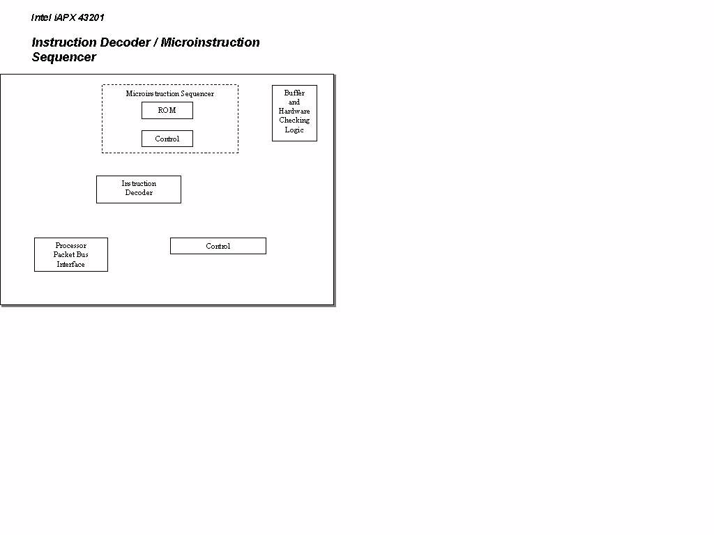
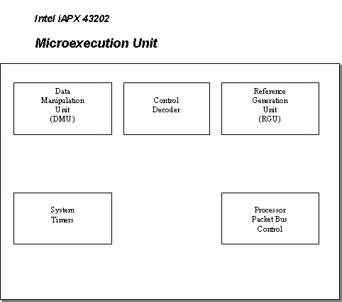
The General Data Processor, comprised of the 43201 and 43202 chips, contains the units for instruction decoding and microinstruction execution (the IDU and MEU respectively). The IDU contains two functional sub-units, an instruction decoder and a microinstruction sequencer (see Figure 3) (I, 161). The MEU contains the two subprocessors mentioned in the register set section, the DMU and the RGU (see Figure 4). The DMU has several functional units: a variable length bit field extractor (a barrel shifter), two double-ended queues, processor state registers, a constant ROM, and two system timers. These functional units allow the DMU to efficiently implement the macroinstruction set. The RGU also contains a number of functional units. These include: four independent stacks, a register array, an adder, an unsigned magnitude comparator, and a content addressable memory (CAM). These units support the virtual memory addressing mechanism of the GDP architecture. To control fixed and variable cycle microinstructions, the DMU and the RGU are equipped with state machines (I, 175-178).
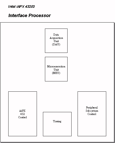
There are two functional units within the Intel 43203 Interface Processor – the data acquisition unit (DAU) and the microexecution unit (MEU) (see Figure 5). Address mapping, data transfer, and access control are controlled by the DAU. The DAU provides up to five windows that access different sections in the main memory of the 432. Interrupt handling and execution take place in the MEU, which is a microprogrammed machine (I, 153). These two functional units, the DAU and the MEU, contain four unique circuits. The DAU has a static CAM and a byte packing buffer. The MEU houses a structure for handling interrupts and a 2K by 16-bit, 2-bit-per cell ROM (I, 183). In more comprehensive detail, the MEU contains the interrupt controller, an address sequencer, the 2K by 16-bit microcoded ROM, a microinstruction bus and decoder, a 16-bit ALU, and all of the internal working registers (I, 187).
The 43201 and 43202 chips that make up the General Data Processor are tightly coupled via a local 16-bit microinstruction bus. The General Data Processor’s MEU has seven major data buses: three of these buses are used by the RGU, three by the DMU, and the last is used as a microinstruction control bus (I, 179). The 43203 Interface Processor also contains a number of buses. These buses include: address, microinstruction, internal ACD, displacement, interrupt address, PS data and PS address (I, 184).
"Both the GDP and the IP are microprogrammed, each containing a 4K by 16-bit and a 2K by 16-bit ROM, respectively" (III, 601). Microcode for the General Data Processor is allocated for several functions including: basic instruction set (6%), floating point arithmetic (10%), run-time environment (10%), virtual addressing (7%), fault handling (4%), silicon OS (40%), multiprocessor control (13%), and debugging services (2%) (I, 179). The microcoded ROM in the IP contains the microprogram that is executed by the chip’s microexecution unit (I, 185).
External busing is facilitated through the Intel Multibus. The Multibus is used as a component in the interrupt-driven I/O processing environment of the iAPX 432 system (I, 171). Each Multibus connects an associated processor (such as an Intel 8086), local memory and I/O devices. The IPs transfer data between Intel 432 memory and Multibus local memory; all I/O is actually performed by the associated processor (VII, 160).
INSTRUCTION FETCH AND EXECUTION
In the iAPX 432, the fetching and executing of instructions is implemented on separate chips. The 43201 is the instruction decoding unit, which fetches and decodes instructions, and the 43202 is the microexecution unit, which executes decoded instructions from the 43201 and then generates addresses for memory accesses (III, 198).
The General Data Processor (GDP) is internally designed as a three-stage microprogram-controlled pipeline. The stages are the instruction decoder, the microinstruction sequencer, and the execution unit. The first two stages are located in the 43201 and the third is in the 43202. The instruction decoder in the 43201 receives macroinstructions, processes variable-length fields, extracts logical addresses, generates starting addresses for the microinstruction sequences, and generates microinstructions for simple operations. The microinstruction sequencer (the second stage of the pipeline) issues microinstructions to the execution unit (the 43202), executes microinstruction sequences out of its ROM, responds to the bus control signals, invokes macroinstruction fetches, and initiates interprocessor communication and fault-handling sequences. The execution unit (the third stage of the pipeline) is made up of two independent subprocessors, the data manipulation unit (DMU) and the reference generation unit (RGU). These subprocessors are controlled by separate sequencers. The reference generation unit handles memory accesses and performs memory mapping, while the data manipulation unit houses the ALU (III, 602-604). The processing units are clocked in two-phases at eight MHz to yield a minimal microcycle time of 125-nsec (III, 601).
To achieve single-cycle microinstruction execution, the MEU in the interface processor was highly pipelined. The MEU pipeline has five stages. In the first stage, interrupt requests and grants take place as well as microaddress computation.
During the second stage, the microcode ROM is accessed. Next, in the third stage, the microinstruction is decoded, the operands are accessed, and the interface signals are sampled. The fourth stage involves data movement and performing ALU operations. In the fifth and final stage, the 432 interface signals are driven. At any given time, there may be up to five microinstructions in different stages of completion in the pipeline (I, 187).
The total physical address size for the iAPX 432 is 224 bytes while the upper limit on the logical address space is 240 bytes. At any given moment, the maximum logical addressing environment for a program is limited to 232 bytes (I, 157). The speed of this memory allows a 32-bit word to be transferred in 250 nanoseconds (I, 165).
A segmented memory layout is used in the iAPX 432. There may be up to 224 (approximately 16 million) segments with each segment being 216 bytes. This gives a total virtual space of 240 bytes (more than one trillion bytes) (III, 488). Segments can be either access segments or data segments (I, 163).
A two-level mapping mechanism is implemented on the 43202. A logical address is translated into a physical address by looking in a segment table for a segment descriptor. The segment descriptor contains the starting physical address, the length of the segment, and the type of the segment (data or access). Using the two-step mapping process, the access descriptor selects the segment descriptor, which then leads to the offset in memory where the data is located. Program modules are given a collection of segment numbers that it may need to access; no other access is allowed. This is the access environment of the module; it is stored in a segment of its own called the access segment. Other segments are data segments that contain the data and instructions of the modules. Modules that try to access segments that are not in its access descriptors produce a fault (III, 488).
The iAPX 432 uses an internal associative cache to decrease the time of the address translation process. The segment descriptors and address descriptors (as well as the addresses of commonly accessed items like the segment table) that were most recently used are all stored on the chip (III, 488). The cache was too small; it improved performance but not enough to compensate for the slow memory accesses caused by error checking and other similar problems (V).
In 1983, the Bus Interface Unit (BIU) (a fourth chip) was introduced to the iAPX 432 system. The BIU was designed for multiprocessor support; it allowed up to 63 modules on a single bus and up to 8 independent buses. This allowed memory interleaving, which helped to speed up memory access (V). This also helped to overcome the problem of bus saturation caused by all processors communicating through one bus (I, 172).
The iAPX 432 uses segment-specific protection and user-specific protection (III, 22). The protections slowed memory access (effectively) as a second memory location often had to be read to verify the access rights of the current process.
SUPPORT FOR SHARING MEMORY BETWEEN PROCESSORS
In the iAPX 432, multiple processors are able to use a common memory bus through the use of the Packet Interconnect Protocol. This protocol allows for separate packets for requests and replies, all of which are of varying lengths to yield maximum bus efficiency. The Packet Interconnect Protocol only details the logical implementation of the bus and so the physical implementation is left to the user. This way, the user can shape the structure of the physical bus to meet needs of the specific application. Data buses can be implemented sixteen, thirty-two, or sixty-four bits wide (I, 171-172).
INTER-PROCESSOR COMMUNICATIONS NETWORKS
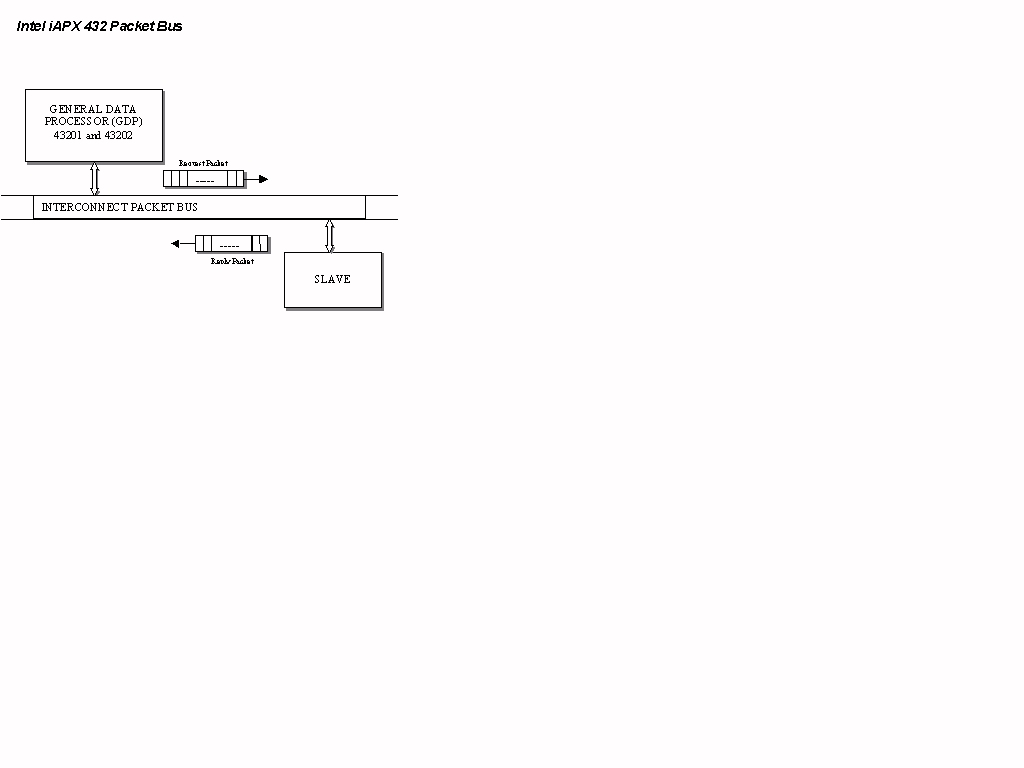
Communication among the General Data Processor, the Interface Processor, and memory takes place via packet-based interconnect bus (III, 601). This interconnect bus functions by sending "packets." By sending these packets, processors are able to communicate with each other as well as with memory. Separate packets are sent for requests and replies; they are variable in length and may contain from one to sixteen bytes of information. Variable length packets make efficient use of the interconnect bus since the bus is only tied up for the time required to send each packet.
To exemplify how the interconnect bus functions, suppose a processor wants to access a slave (see Figure 6). This processor would generate a request packet (which would include items such as an address, byte count, type of request, etc.) and put it out on the interconnect bus. The processor would then expect a reply packet to come back from the slave if the request specified a read cycle. If a read operation were requested, the slave would respond by sending a reply packet to the processor once it was ready. In the interval between the sending of the request and the sending of the reply packet, other processors are able to use the interconnect bus. An even greater level of efficiency can be achieved by widening the interconnect bus (III, 213-214).
Communication between processors and memory, as well as between multiple processors, uses a single bus. Therefore even a small number of processors quickly causes the bus to become saturated, which greatly slows the system (I, 172).
I/O is performed by processor subsystems, which provide intelligent, independent, and decentralized I/O for the iAPX 432. These subsystems can process concurrent I/O requests and can initiate them as well (I, 171). The subsystems communicate with the 432 via the Interface Processor (IP), the 43203. The IP provides I/O facilities that are fully independent and decentralized. It also maps a portion of the peripheral subsystem address space into the system memory. A peripheral subsystem is an independent microcomputer system that has its own local memory, I/O devices and controllers, at least one conventional processor (such as an 8086), called the attached processor (AP), and software. Together the IP and the AP form the logical I/O processor of the iAPX 432 system. All peripherals are interfaced to the interrupt-driven I/O subsystem bus (Multibus). The IP is able to communicate with I/O devices via executing various tasks, including device driver execution, device interrupt handling, and DMA channel initialization. The IP also has the ability to detect hardware errors. Multiple IPs may be connected to a 432 system, each one able to attach one peripheral subsystem to the main iAPX 432 system (III, 608).
The 43203, the Interface Processor, acts as the system channel for I/O by extending the object and instruction set of the 432 system and therefore allowing programs the ability to communicate to other subsystems through an external interface. The IP allows an I/O processor to move data into and out of the 432 memory through executing a subset of the 432 operations; it also extends the protection model to the external interface. In other words, external devices can only write into specific objects designated by the respective 432 process (II, 344).
The speed of the I/O devices is determined by the type of device and the type of chip used in the subsystem.
Speed was one of the main problems of the iAPX 432. Running at 8 MHz, both the iAPX 432 and the 80286 were compared with the following results:
(Using 16-bit words, all times in milliseconds)
| Processor | Search | Sieve | Puzzle | Ackerman |
| iAPX 432 | 4.4 | 978 | 45700 | 47800 |
| 80286 | 1.4 | 168 | 9138 | 2218 |
(I, 166)
The iAPX 432 was approximately 1/4 the speed of the 80286 for most applications; it was slower than most of the processors that were available at the time of its release by at least 10% (I, 166). The causes of the speed problems were the lack of user registers, the data protection routines, the need for separation of tasks onto more than one chip, the massively complex microcoded control unit, and its too-small cache (VI).
All of the iAPX 432 system components are capable of running in a Functional Redundancy Mode. This is used to configure out bad nodes when errors occur during a cycle (I, 172). The Memory Control Unit (MCU) was introduced to the iAPX 432 in 1983, along with the BIU. The MCU performed automatic parity checking as well as ECC error checking. The iAPX 432 was designed to be fault tolerant; this was helped by the addition of the MCU (V).
Interrupt control logic is implemented in the IP with a structure called the storage logic array (SLA). Interrupts are processed according to priority. Interrupts can only be interrupted by interrupts of higher priority. An interrupt is handled by microcoded routines via creating an interrupt process and sending it to a dispatch port with the appropriate priority. I/O interrupts are caught by the aforementioned I/O system and handled, often without interrupting the processor (I, 187-188).
The iAPX 432 was more of a learning experience for Intel than anything else. There were many things learned from the 432, including how to do multiprocessing and multiprogramming, how to best create processors for large-scale applications in critical areas, how to implement dependability (fault tolerance), and how to use CISC to ease the burden of programming for assembly programmers and compilers. The 432 used several modern computing concepts, mainly the idea of direct memory access for I/O and the concept of the virtual machine. The things learned by Intel were later applied to many successful processors, most notably the 960 series and x86 architectures. The Pentium Pro, the 960, and the 432 had the same lead architect: Fred Pollack. The 960 series are embedded processors but they retain the ability to run well with Ada (V).
The iAPX 432 was a flop and was discontinued only four years after its release. Speed was the main reason that the processor failed, although many programmers did not see Ada as the way of the future and therefore ignored the chip. The reason the 432 was so slow was that it verified many memory accesses (causing a memory read), its instructions were not aligned and took a while to decode, it did not have a large enough cache, it did not have enough registers, and it had extra chips which had to communicate. The success of the 80286 sealed its fate; as mentioned above it was four times faster than the 432. The iAPX 432 taught Intel a lot about what could and could not be done, and it was impressive that such a complex a system could be created with the available technology, but it was too complicated for practical use.
(I) Amar Gupta and Hoo-Min Toong, "Advanced Mircoprocessors," New York, N.Y., IEEE Press, 1983. pp. 153-157, 160-167, 170-173, 175-178, 183-188, 242
(II) Glenford J. Myers, "Advances in Computer Architecture," John Wiley & Sons, New York, N.Y., 1982. pp. 344, 335-340, 366, 371
(III) Nikitas A. Alexandridis, "Microprocessor System Design Concepts," Computer Science Press, Rockville, M.D., 1984. pp. 22, 26, 198, 213-214, 488, 601-608
(IV) S. Zeigler, N. Allegre, R Johnson, J. Morris, "Ada for the Intel 432 Microcomputer," Computer, Vol. 14 Number 6, June 1981, pp. 47-56
(V) John Bayko, "Weird and Innovative Chips," Great Microprocessors of the Past and
Present, http://194.226.182.114/microprocessor/great/s6.html
(VI) John C. Dvorak, "Whatever Happened to Intel’s Dream Chip?," Computer Shopper, http://computershopper.zdnet.com/texis/cs/doframe.html?rg=r129&u=www.zdnet.com/computershopper/edit/cshopper/filters/punwha.html
(VII) Henry Levy, "Capability-Based Computer Systems," Digital Press, Bedford, M.A., 1984. pp. 160