DEC COMPUTER LAB
DEC's COMPUTER LAB was a hands-on digital logic trainer. It provided
gates, flip-flops, a clock source, switch inputs, and lamp outputs. The
user wired it with patch cords.
I don't have a COMPUTER LAB, but I'd love to get one. If you have one,
or know where I might get one, please
email me.
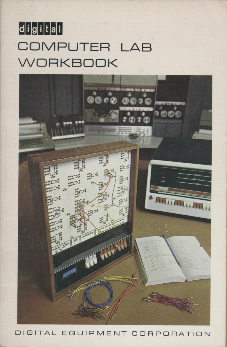
Here are the front and rear covers of the COMPUTER LAB WORKBOOK
dated April 1969.
Click on the images for larger versions.
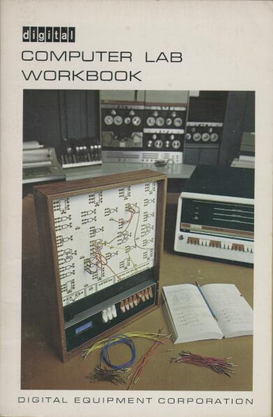
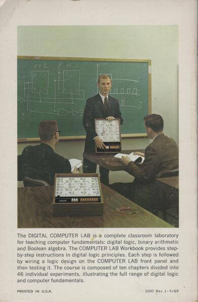
Table of Contents
- PREFACE
- INTRODUCTION
- OPERATING INSTRUCTIONS
- CHAPTER 1 The Binary Concept
- Experiment 1.1: 2-Input NAND Gate
- Experiment 1.2: 3-Input NAND Gate
- Experiment 1.3: 4-Input NAND Gate
- Experiment 1.4: Inverter
- Experiment 1.5: Substituting Gates
- Experiment 1.6: Decimal to Binary Encoder
- Experiment 1.7: Binary to Decimal Decoder
- CHAPTER 2 Basic Logic Gates
- Experiment 2.1: AND/NOR Gate
- Experiment 2.2: NOR Gate Application of AND/NOR Gate
- Experiment 2.3: AND/NOR Comparator
- Experiment 2.4: AND/NOR Gate Used for Exclusive OR
- Experiment 2.5: Non-Inverting Gate
- Experiment 2.6: Equality Detector
- Experiment 2.7: Parity Bit Generator
- CHAPTER 3 Flip-Flops
- Experiment 3.1: R-S Flip-Flop
- Experiment 3.2: Clocked R-S Flip-Flop
- Experiment 3.3: D Type Flip-Flop
- Experiment 3.4: J-K Flip-Flop
- Experiment 3.5: 4-Bit Shift Register
- CHAPTER 4 Boolean Algebra to Gating Networks
- Experiment 4.1: Gating Circuit Simplification
- Experiment 4.2: Equality and Relative Magnitude Detector
- CHAPTER 5 Binary Counters
- Experiment 5.1: Asynchronous Binary Up Counter
- Experiment 5.2: Modified Asynchronous Binary Counter
- Experiment 5.3: Synchronous Binary Up Counter
- Experiment 5.4: Synchronous Binary Up/Down Counter
- Experiment 5.5: Synchronous Modulo 6 Binary Up Counter
- Experiment 5.6: Asynchronous Self-Stopping Modulo 13 Binary Counter
- Experiment 5.7: Variable Modulus Asynchronous Binary Up Counter
- CHAPTER 6 Serial Addition
- Experiment 6.1: Serial Adder
- Experiment 6.2: Subtraction Using the Serial Adder
- Experiment 6.3: Multiplication Using the Serial Adder
- CHAPTER 7 Parallel Addition
- Experiment 7.1: Parallel Adder
- Experiment 7.2: Two's Complement Subtraction
- Experiment 7.3: One's Complement Subtraction
- Experiment 7.4: One Step Parallel Addition
- CHAPTER 8 Binary Coded Decimal Operations
- Experiment 8.1: The 8421 Counter
- Experiment 8.2: The Excess 3 Counter
- Experiment 8.3: The 2421 Counter
- Experiment 8.4: The 5421 Counter
- Experiment 8.5: Serial BCD Addition
- CHAPTER 9 Code Conversion and Decoding
- Experiment 9.1: The 2421 to 8421 Converter
- Experiment 9.2: The 5421 to 8421 Converter
- Experiment 9.3: Gray to Binary Converter
- CHAPTER 10 System Considerations
- Experiment 10.1: Parallel Adder Control
- Experiment 10.2: Synchronizers
- Experiment 10.3: Maximum Frequency
- Appendix A: Checkout Procedures
- Appendix B: Karnaugh Mapping
- Appendix C: TTL Circuitry
- Appendix D: The Computer
- Appendix E: Glossary of Terms
- Appendix F: Decimal to Binary Conversion Table
- Appendix G: Powers of Two
- Appendix H: Recommended Texts
- Appendix I: COMPUTER LAB Hardware Specifications
- Appendix J: Warranty
- Appendix K: Logic Element Truth Tables
APPENDIX I
COMPUTER LAB HARDWARE SPECIFICATIONS
- I
- GENERAL SPECIFICATIONS
- 1.
- Size -- 16 1/2" x 12 1/2" x 3 1/4" (cases are stackable).
- 2.
- Finish -- Simulated teak.
- 3.
- Power Requirements -- H500: 50 or 60 cps, 105 to 120 VAC;
H500A: 50 or 60 cps, 210 to 240 VAC.
- 4.
- Power Switch -- On Variable Clock Control.
- II
- ELECTRONIC LOGIC SPECIFICATIONS
- 1.
- Functions Available:
8 J-K Flip-Flops (Master-Slave type)
8 2-Input NAND Gates
6 3-Input NAND Gates
4 4-Input NAND Gates
4 AND/NOR Gates
- 2.
- Type of Circuits:
Transistor-Transistor Logic Integrated Circuits
- 3.
- Logic Levels:
HI -- +3 volts nominal (+2.4 to +3.6 volts)
LO -- Ground nominal (0.0 to +0.4 volts)
Internal Supply Voltage: +5 volts (not available on patch panel)
- 4.
- Input Loading:
Unit Load: 1.6 ma at GND. +40 µa at +3 volts.
Gate inputs and Flip-Flop J & K inputs present one load each.
Flip-Flop Clock and Reset inputs present two loads each.
Lamp Indicator inputs present five loads each.
- 5.
- Output Drive:
The Fan-Out of an output indicates the number of unit loads that output can drive:
Logic outputs on the patch panel have a fan-out of 10.
Rocker Switches, Pulsers, teh Clock, and HI terminals have a fan-out of 30.
- III
- CONTROL AND INDICATOR SPECIFICATIONS
- 1.
- Functions Available:
8 Rocker Switch logic level generators
3 Pulser Switches
8 Lamp Indicators
1 Variable Frequency Clock
- 2.
- Rocker Switches:
Give HI output when upper side of switch is depressed.
Give LO output when lower side of switch is depressed.
Fan out: 30.
- 3.
- Pulser Switches:
Normally provide a LO output.
HI output when depressed, reamin HI until released.
Fan-out: 30.
Build-in switch filters.
- 4.
- Lamp Indicators:
Normally OFF when no input.
ON when corresponding input HI.
OFF when corresponding input LO.
Load: 5 unit loads.
- 5.
- Clock:
Repetition rate: less than 1 pulse per second to more than 10 x 106 pulses per second.
Pulse width: 50 nanoseconds nominal.
Fan-out: 30.
 Back to my retrocomputing page
 Back to my home page
Last updated November 15, 1998
Copyright 1998 Eric Smith
eric@brouhaha.com
 check now