Reprinted from Intelligent Machines Journal Issue 5, March 14, 1979, page 22
Microprocessors will be able to achieve much higher performance in a new package developed by Intel Corporation and 3M Company for use by Intel and other semiconductor manufacturers.
Named the “Quad In-Line Package” (QUIP), the new 64-pin design complements advances in large-scale integration technology that have made it practical to produce high-performance microprocessors with functional densities of 50,000 to 100,000 transistors per semiconductor chip.
The QUIP will also help make further advances in LSI technology usable in the future, according to Intel. Although more economical and almost twice as compact as a conventional dual in-line package (DIP) design with 64 pins, the QUIP allows a much larger, higher density, faster device to be packaged.
Intel claims that the QUIP is also superior both to the 40-pin DIPs generally used to package microprocessors and to a new 68-pin square package aimed primarily at computer applications requiring high-density multilayer boards. Moreover, the QUIP can cover both DIP and square package applications ranges. That is, it can be used efficiently both on low-cost, two-sided wiring boards and on multilayer boards.
Intel’s Microcomputer Components Division initiated the joint development effort with 3M Company because the semiconductor industry did not have a package suitable for microprocessors requiring more than 40 pins.
3M Company, which also produces DIPs and square packages, will supply the QUIP to the semiconductor industry at large. The QUIP will be priced to compete with DIPs, and is expected to cost less than a 64-pin DIP, when bought in large quantities.
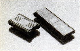
The Quad In-Line Package is actually a miniature, 64-pin packaging system for very large and very fast semiconductor devices with power dissipation up to 2 watts or more. It provides a larger cavity for the chip, better electrical performance, and much lower thermal resistance than conventional packages, according to Intel.
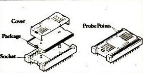
The semiconductor chip is sealed in a leadless ceramic package that fits “upside down” into its socket, and is cooled from the top by a metal cover. The metal cover also clips the package into the socket. The socket has four rows of pins instead of two rows (quad instead of dual-in-line) to keep the package compact and boost its electrical performance.
3M Company will soon make available both an optional high-temperature socket for device burn-in processing, and a clip-in cable connector for system development and diagnostic aids.
The new construction improves all key specifications that govern circuit complexity and performance — cavity size, thermal resistance, pin-to-pin capacitance, and lead electrical resistance — as well as providing the additional pins needed to expand microprocessor architectures.
Although the QUIP’s specifications came from an Intel engineering study of trends in the packaging requirements of microprocessors and single-chip microcomputers, it can also meet the requirements of other major logic components, such as “intelligent” peripheral controllers, which are also heading toward very high functional densities.
The QUIP has the largest cavity of any available package — 400 mils square by 25 mils deep — to assure ample room for packaging very large devices with high pin counts.
It also has a lower thermal resistance — only 35 C per watt compared with 60 to 90 C per watt for 64-pin DIPs. The reduction will allow a QUIP-packaged chip to dissipate over 2 watts of power in still air without exceeding a junction temperature of 170 C (the safe internal temperature of an advanced MOS device).
“Thermal resistance was our main concern because it dictates functional density. The more transistors operating on a single chip, the more power the chip must be able to dissipate,” explained William Lattin, an Intel microcomputer engineering manager.
Pin-to-pin capacitance is lower than a 40-pin DIP’s. The reduction will allow QUIP-packaged devices to operate at higher speed. Capacitance is approximately 3 picofarads, less than half that of some 64-pin DIPs. Lead resistance is less than 0.5 ohm.
The QUIP and DIP can both be used efficiently on low-cost two-sided boards with package pins laid out at 100 mils spacing. This layout is used by most manufacturers of microprocessor-based systems.
Moreover, the QUIP can also be used efficiently — like flat packages and square packages — on multilayer boards with high-density wiring spaced at 50 mils. This dual capability will allow microprocessor manufacturers to standardize on a single package for all applications, from single chip microcomputers for low-cost systems to high-performance microprocessors for high-end microcomputer or computer systems, Intel says.
The QUIP’s pins are spaced at 50 mils in each row and the rows are staggered by 50 mils. As a result, wiring can run in parallel at 50-mil spacing to all pins on a single layer or on multiple layers, or it can run in parallel at the 100-mil spacing if half the pins are connected on each side of the board. All 64 pins fit into a standard hole grid (50-mil grid normally used for automatic hole drilling).
The QUIP incorporates other features designed to make it easier and more economical to use.
The integral socket eliminates mounting and insertion problems. No force is required to insert or to remove the package.
When the metal cover is clipped on, it presses the ceramic package’s printed contacts down onto spring-loaded contact pins in the socket. When the cover is snapped off, the ceramic package is released from the socket.
The printed contacts are brought around to the other side of the package (the ceramic substrate carrying the chip upside down) so that electrical tests can be made after assembly by simply applying probes to the top of the package while the part is operating. The metal cover clears the test contacts so operating tests can be made with the cover holding the device in place.
Cooling is easy; since the substrate faces up, heat flows naturally up from the chip to the cover, which dissipates it into the air. To enhance cooling, the cover has slots which act as cooling fins, stamped in each end.
To prevent human errors in system assembly and maintenance, the package is completely polarized. The socket can only be plugged into the circuit board in one direction because of the staggered pin organization. Also, the socket is keyed to accept the ceramic package in only one way.
The QUIP costs less to make than a 64-pin DIP because it is smaller and eliminates the conventional lead frame. However, the QUIP offers even larger savings in semiconductor manufacturing and system costs.
At the semiconductor plant, the ceramic package is designed to provide a high-strength chip carrier for automated chip bonding, sealing, and testing. It eliminates the lead bending, lead damage, and package breakage problems associated with large DIPs.
At the system level, it saves some 40% of board area compared with a 64-pin DIP. It is almost as compact as a 40-pin DIP — it’s wider, but shorter. Also, the QUIP requires less board area than a 64-pin square package.
The greatest system savings are expected to accrue in applications where sockets must be used to facilitate system development or maintenance. Most such techniques require that the microprocessor be removed from and returned to the socket frequently. A conventional package with a large number of pins is difficult to socket because it requires high insertion forces and careful alignment while being pressed into the socket.
Intel also claims a more efficient use of board real estate with the QUIP. Although a square package uses less board area than a QUIP or DIP, the square design suffers from board layout problems on low-cost, two-sided boards. When package interconnects are included in the board area, the total board area is greater due to the interconnect layout problem. Also, sockets are not yet available for square packages.
Contact Intel Corporation, 3065 Bowers Avenue, Santa Clara, CA 95051; (408) 249-8027.